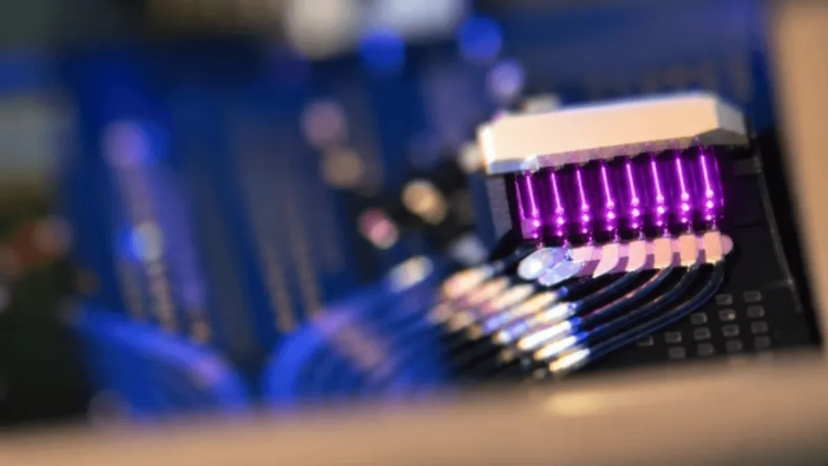
An emerging challenge threatens to constrain AI infrastructure growth: the shortage of lasers needed to interconnect massive processor clusters. Photon Bridge, based in Eindhoven, has just closed a €10 million funding round to solve this bottleneck by creating scalable laser technology purpose-built for data centre deployment.
The investment was jointly led by newcomers Amadeus APEX Technology Fund and 360 Capital, alongside returning backers Innovation Industries, Faber, and Brabant Development Agency (BOM), who all increased their stakes.
Industry analyst Omdia projects that annual shipments of AI accelerators for data centres will exceed 20 million units by 2028. As AI systems expand from thousands to hundreds of thousands of processors operating in tandem, the ability to move data between chips has emerged as a critical performance limitation.
Optical links offer substantial advantages over traditional electrical connections, delivering faster data transfer with greater energy efficiency. The technology is progressively moving nearer to processors themselves, particularly through co-packaged optics—a technique that places optical components directly adjacent to the chips managing data flow within AI systems.
This architectural shift, however, introduces a new constraint: the photonics industry must dramatically increase laser production capacity. The current high-power laser ecosystem was developed primarily for telecommunications and undersea cable applications, where manufacturing volumes remain comparatively modest. Transitioning to AI-scale production means treating lasers as semiconductor-class components rather than specialty photonics devices.
Photon Bridge's engineering strategy reflects this reality. Rather than relying on a limited number of increasingly powerful lasers, the company multiplexes light from several lower-power semiconductor lasers. This distributed approach reduces power density per laser, making individual units less vulnerable to manufacturing imperfections and enabling higher production yields—essential as volumes climb.
The platform targets delivery of numerous wavelength channels, providing up to 40 mW of optical power per wavelength per fibre, while supporting fabrication across multiple indium phosphide (InP) foundries.
AI is fundamentally changing the way computing infrastructure is built. We are moving towards enormous systems in which hundreds of thousands of processors have to operate together, and moving data between them is becoming one of the defining constraints on performance. That means optics has to move closer to the compute. But it also creates an entirely different manufacturing challenge. The industry will soon need millions of these laser sources every year. Instead of making individual lasers increasingly powerful and difficult to manufacture, we move that scaling challenge into the architecture.
Paul Marchal, CEO of Photon Bridge
Manufacturing yield sits at the centre of Photon Bridge's strategy—a factor that grows increasingly critical as laser fabrication transitions from traditional telecom scales to the volumes demanded by AI infrastructure.
Every new wave of compute creates new bottlenecks further down the supply chain, and lasers are the next one. Photon Bridge is addressing this with a technology that combines deep photonics expertise with a credible path towards manufacturing at very large scale.
Ion Hauer, Investment Partner at APEX Ventures
AI is turning lasers from a telecom component into a semiconductor-scale product. Once you start talking about millions of units a year, manufacturing yield becomes fundamental. Photon Bridge has designed its architecture from the beginning around the volumes this market is going to require.
Cesare Maifredi, Partner at 360 Capital
The capital infusion will enable Photon Bridge to expedite engineering work and customer testing, with initial production samples targeted for 2027 and full-scale manufacturing commencing in 2028. The company plans to expand its Eindhoven workforce as it moves toward market entry.
Source: Tech.eu